One of the most common questions we get at Epilog is "can your lasers do printed circuit boards?" The answer is multifaceted and, depending on the application, there are some ways to use lasers with PCBs. Here we'll take a look at the some PCB applications suited for a laser as well as those that are not.
Printed circuit boards (PCB) are most often found in a variety of electronic devices. They support and electrically connect electronic components using conductive pathways, tracks or signal traces etched from copper sheets and then laminated onto a non-conductive substrate, such as G10 or FR4.
The vast majority of printed circuit boards are made by bonding a layer of copper over the entire substrate, then removing unwanted copper after applying a temporary mask (by etching), leaving only the desired copper traces.
Depending on the desired outcome, Epilog Laser systems can be used in various capacities in the PCB realm. Here we'll take a look at some different PCB applications and how they relate to the laser.
Ideal laser PCB applications:
1) Cutting tabs on sheets of ready-made PCBs.
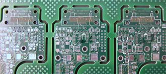
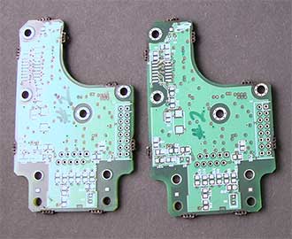
The images below illustrate a sheet of already created circuit boards. Operators can use an Epilog Laser system to cut tabbed perforations around each board out so they can be easily removed from the sheet.
Best type of laser for this appliation: Fiber Laser.
While Epilog's CO2 systems will cut through the PCB as long as there is no copper layer, our fiber laser systems (the FiberMark 24 and Fusion M2 Fiber Laser) will cut through both with and without the copper layer.


2) Marking graphics/text on pre-made PCBs.
If you are looking to mark a printed circuit board with a bar code, logo, or serial number, this is also possible with our laser systems.
Best system for this appliation: CO2 Laser or Fiber Laser.
When marking directly on a PCB we are able to achive a low-contrast mark with both our fiber and CO2 laser systems. This is an application we would want to test with the PCB you will be using in our Applications Lab to make sure it fit your needs.
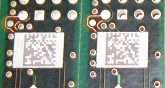
Many PCBs are designed with a variety of components. The PCB to the right contains a white area of engineered plastics that works well for barcodes, QR codes, or in this case, data matrix codes.
This 2D data matrix code was processed using a CO2 laser from Epilog. Our fiber laser was also able to mark the same white layer, however did not result in as much contrast.

3) Engraving Through PCB material to expose copper layer.
Epilog's FiberMark and Fusion M2 Fiber Lasers are able to engrave through PCB material to expose the copper layer underneath. Because the layer is so thin, the fiber lasers can also cut through that material.
While some PCB applications are laser friendly, others are better suited to a different kind of technology. The following PCB applications do not lend themselves to being completed using the laser.
1. Exposing copper
The laser, specifically the FiberMark and Fusion FiberMark systems, can etch away the surface material to expose the copper beneath; however, even though it is exceptionally precise, there can still be trace amounts of PCB material left behind. It can be challenging to ensure you get the exact amount of copper exposure you need.
2. Cutting PCBs with a CO2
Because the CO2 lasers cannot directly etch metal or cut it, we don't recommend cutting PCBs with this type of laser.